本文主要是介绍ADUCM331开发笔记(一)GPIO的使用与Blinky例程,希望对大家解决编程问题提供一定的参考价值,需要的开发者们随着小编来一起学习吧!
ADUCM331开发笔记(一)GPIO的使用与Blinky例程
- ADUCM331开发笔记(一)GPIO的使用与Blinky例程
- GPIO的使用说明
- GENERAL-PURPOSE DIGITAL INPUTS/OUTPUTS OVERVIEW
- GENERAL-PURPOSE DIGITAL INPUTS/OUTPUTS FEATURES
- GENERAL-PURPOSE DIGITAL PORT MULTIPLEX
- GENERAL PURPOSE DIGITAL INPUT/OUTPUT OPERATION
- Digital Port Multiplexed Configuration多种模式配置
- GPIO Pull-Up Enable上拉使能
- GPIO Data In输入
- Open Circuit Enable开路使能
- GPIO Data Out输出
- Bit Set位置位
- Bit Clear位清零
- Bit Toggle位翻转
- GPIO Data Output Enable输出使能
- GPIO MEMORY MAPPED REGISTERS寄存器列表及其内存映射
- GPIO Configuration Register配置寄存器GP0CON
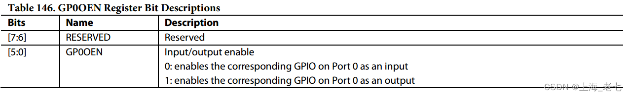
- GPIO Output Enable Register输出使能寄存器GP0OEN
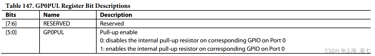
- GPIO Output Pull-Up Enable Register上拉使能寄存器GP0UPL
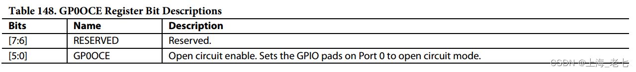
- GPIO Open Circuit Enable Register开路使能寄存器GP0OCE
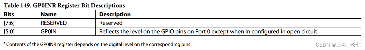
- GPIO Input Data Register输入数据寄存器GP0INR
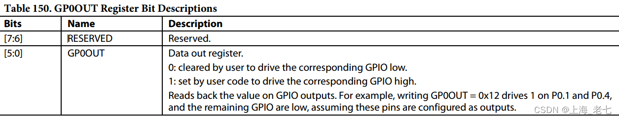
- GPIO Data Out Register输出寄存器GP0OUT
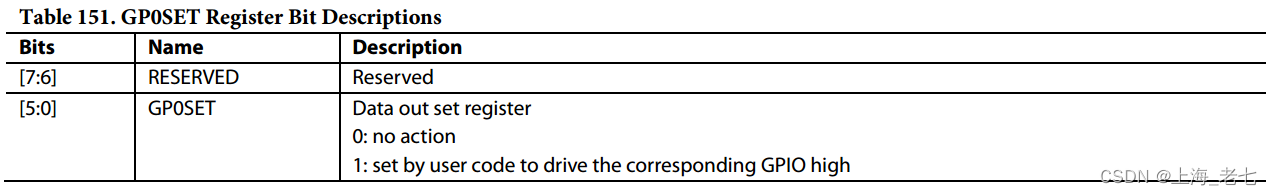
- GPIO Data Out Set RegisterGP0SET输出置位寄存器GP0SET
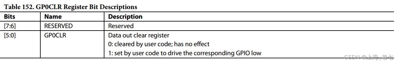
- GPIO Data Out Clear Register输出清零寄存器GP0CLR
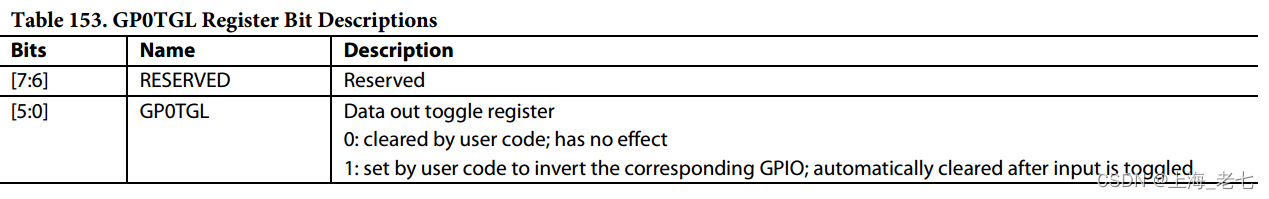
- GPIO Pin Toggle Register输出翻转寄存器GP0TGL
- Blinky例程代码
- RTE设置
- RTE代码
- 芯片头文件
- 绝对地址使用
- GPIO初始化设置
- 中断时钟
- 中断处理函数
ADUCM331开发笔记(一)GPIO的使用与Blinky例程
ADUCM331开发笔记,记录每天的进展。
GPIO的使用说明
ADuCM330/ADuCM331 Hardware Reference Manual UG-716
GENERAL-PURPOSE DIGITAL INPUTS/OUTPUTS OVERVIEW
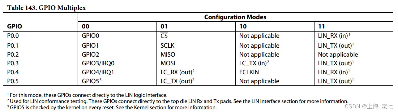
The ADuCM330/ADuCM331 feature six, bidirectional, general-purpose input/output (GPIO) pins. All of the GPIO pins have multiple
functions, configurable by user code. These features are described in Table 143.
Each GPIO pin can be configured as an input, output, or open circuit. These pins also have an internal, pull-up, programmable resistor.
See the ADuCM330/ADuCM331 data sheet for logic input voltages and absolute maximum values. For optimum low power operation,
the GPIOs must be configured as inputs (using GP0OEN) and with pull-up resistors enabled (using GP0PUL).
When the ADuCM330/ADuCM331 enter a power saving mode, the GPIO pins retain their state.
Note that a driving peripheral is not able to drive these pins.
GENERAL-PURPOSE DIGITAL INPUTS/OUTPUTS FEATURES
• Six, bidirectional, general-purpose input/output (GPIO) pins
• Internally multiplexed with SPI and LIN configurations available
GENERAL-PURPOSE DIGITAL PORT MULTIPLEX
This block provides control over the GPIO functionality of specified pins, because some of the pins can work as GPIOs or have other
specific functions. The following tables detail the configuration modes for each GPIO.
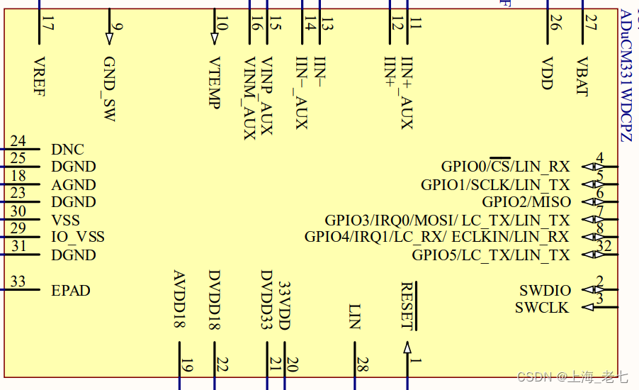
某产品GPIO电路如下,可见该产品的GPIO没有使用。如果后续需要使用GPIO0口,即Pin4,作为一路数字量输入,则需要电路上稍作变更,并把GPIO0的Configuration Modes设置为00。
GENERAL PURPOSE DIGITAL INPUT/OUTPUT OPERATION
Digital Port Multiplexed Configuration多种模式配置
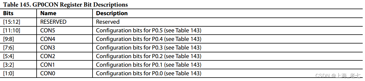
The pin functions are configured using the GP0CON register. The GP0CON register configures Port 0. External interrupts and input level signals (GP0IN) are available in any configuration modes, except when the GPIOs are configured as open circuit and as outputs (GP0OE = 1 and GP0OCE = 1).
引脚功能使用 GP0CON 寄存器进行配置。GP0CON 寄存器配置端口 0。除非 GPIO 配置为开路和输出 (GP0OE = 1 和 GP0OCE = 1)之外,其他任何配置模式中外部中断和输入电平信号 (GP0IN) 均可用
GP0CON寄存器用于配置Port0,包括P0.0到P0.5六个Pin脚。
GPIO Pull-Up Enable上拉使能
All GPIO pins have an internal pull-up resistor. Using the GP0PUL register, it is possible to enable/disable pull-up registers on the pins
when they are configured as inputs. The pull-up resistors are automatically disabled when the pad is set as an output or when open circuit
is enabled.
所有 GPIO 引脚都有一个内部上拉电阻。当引脚配置为输入时。使用 GP0PUL 寄存器可以启用/禁用引脚上的上拉寄存器。当引脚设置为输出或开路时,上拉电阻自动禁用。
GPIO Data In输入
When configured as an input (by default), the GPIO input levels are available in GP0IN.
Open Circuit Enable开路使能
This disables the input paths if the pin is set as output. To disable the input and not drive the pin, the open circuit must be set and drive
Logic 1. External interrupts interrupt are not available when open circuit is enabled.
GPIO Data Out输出
When the GPIOs are configured as outputs, the values in GP0OUT are reflected on the GPIOs.
Bit Set位置位
Bit set is used to set one or more GPIO data outputs without affecting others within a port. Only the GPIO corresponding with the write
data bit equal to one is set; the remaining GPIOs are unaffected.
Bit Clear位清零
Bit clear is used to clear one or more GPIO data outputs without affecting others within a port. Only the GPIO corresponding with the
write data bit equal to one is cleared; the remaining GPIOs are unaffected.
Bit Toggle位翻转
Bit toggle is used to toggle one or more GPIO data outputs without affecting others within a port. Only the GPIO corresponding with the
write data bit equal to one is toggled; the remaining GPIOs are unaffected.
GPIO Data Output Enable输出使能
The data output path is enabled; the values in GP0OUT are reflected on the GPIOs.
GPIO MEMORY MAPPED REGISTERS寄存器列表及其内存映射
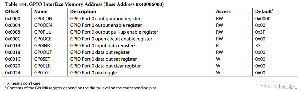
GPIO Configuration Register配置寄存器GP0CON
Address: 0x40006000, Reset: 0x0000, Name: GP0CON
默认模式都设置为00。
GPIO Output Enable Register输出使能寄存器GP0OEN
Address: 0x40006004, Reset: 0x00, Name: GP0OEN
默认都设置为输入
GPIO Output Pull-Up Enable Register上拉使能寄存器GP0UPL
Address: 0x40006008, Reset: 0x3F, Name: GP0PUL
0x3F = 0B 0011 111103,默认使能上拉电阻
GPIO Open Circuit Enable Register开路使能寄存器GP0OCE
Address: 0x4000600C, Reset: 0x00, Name: GP0OCE
GPIO Input Data Register输入数据寄存器GP0INR
Address: 0x40006014, Reset: 0xX1, Name: GP0INR
GPIO Data Out Register输出寄存器GP0OUT
Address: 0x40006018, Reset: 0x00, Name: GP0OUT
GPIO Data Out Set RegisterGP0SET输出置位寄存器GP0SET
Address: 0x4000601C, Reset: 0x00, Name: GP0SET
GPIO Data Out Clear Register输出清零寄存器GP0CLR
Address: 0x40006020, Reset: 0x00, Name: GP0CLR
GPIO Pin Toggle Register输出翻转寄存器GP0TGL
Address: 0x40006024, Reset: 0x00, Name: GP0TGL
Blinky例程代码
Blinky.c主函数比较简单
// includes
#include "RTE_Components.h"             // Component selection
#include <absacc.h>const unsigned int iPage0CS[2] __at(0x07f8) = {0xffffffff,0x16400000};	// for direct startup from Kernel
void GPIO_INIT(void);
//=====================================================================
// 						main
//=====================================================================
int main (void)
{T3CON = 0;  								// Turn off watchdogGPIO_INIT();SysTick_Config(0x320000);while(1){}
}
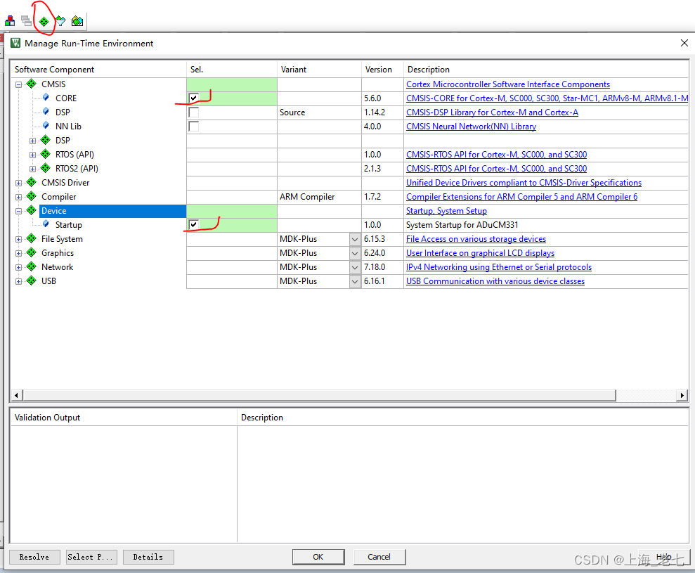
RTE设置
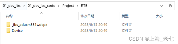
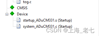
前面包含"RTE_Components.h" ,这个文件是通过下列设置自动添加到路径、并且复制实体文件到的。
RTE代码
主要是引用芯片头文件
#ifndef RTE_COMPONENTS_H
#define RTE_COMPONENTS_H/** Define the Device Header File: */
#define CMSIS_device_header "ADuCM331.h"/* AnalogDevices::Device:Startup:1.0.0 */
#include <ADuCM331.h>#endif /* RTE_COMPONENTS_H */
芯片头文件
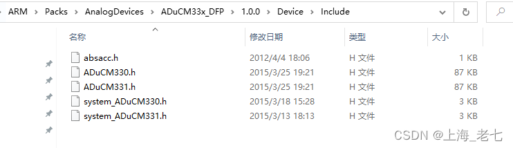
ADuCM331.h文件位置在Keil安装目录下,导入芯片Pack包的时候复制过去的。
打开芯片头文件ADuCM331.h,可以看到GPIO寄存器的名称和地址定义。
// GPIO#define          GPIOBASE                                   (*(volatile unsigned long      *) 0x40006000)
#define          GPIOBASE_A                                 0x40006000
// GPIO Port 0 configuration
#define          GP0CON                                     (*(volatile unsigned short int *) 0x40006000)
#define          GP0CON_A                                   0x40006000
// GPIO Port 0 output enable
#define          GP0OEN                                     (*(volatile unsigned char      *) 0x40006004)
#define          GP0OEN_A                                   0x40006004
// GPIO Port 0 output pull up enable
#define          GP0PUL                                     (*(volatile unsigned char      *) 0x40006008)
#define          GP0PUL_A                                   0x40006008
// GPIO Port 0 open circuit enable
#define          GP0OCE                                     (*(volatile unsigned char      *) 0x4000600C)
#define          GP0OCE_A                                   0x4000600C
#if           ALLOW_DEPRECATED_NAMES
// "GP0ODE" has been deprecated. Use "GP0OCE" instead.
#define          GP0ODE                                     (*(volatile unsigned char      *) 0x4000600C)
#define          GP0ODE_A                                   0x4000600C
#endif
// GPIO Port 0 input data
#define          GP0INR                                     (*(volatile unsigned char      *) 0x40006014)
#define          GP0INR_A                                   0x40006014
// GPIO Port 0 data out
#define          GP0OUT                                     (*(volatile unsigned char      *) 0x40006018)
#define          GP0OUT_A                                   0x40006018
// GPIO Port 0 data out set
#define          GP0SET                                     (*(volatile unsigned char      *) 0x4000601C)
#define          GP0SET_A                                   0x4000601C
// GPIO Port 0 data out clear
#define          GP0CLR                                     (*(volatile unsigned char      *) 0x40006020)
#define          GP0CLR_A                                   0x40006020
// GPIO Port 0 pin toggle
#define          GP0TGL                                     (*(volatile unsigned char      *) 0x40006024)
#define          GP0TGL_A                                   0x40006024
#if           ALLOW_DEPRECATED_NAMES
// "GP0TOG" has been deprecated. Use "GP0TGL" instead.
#define          GP0TOG                                     (*(volatile unsigned char      *) 0x40006024)
#define          GP0TOG_A                                   0x40006024
#endif
绝对地址使用
头文件absacc.h定义了绝对地址的调用语法。
#ifndef __at
#define __at(_addr)  __attribute__ ((at(_addr)))#endif#ifndef __section
#define __section(_name)  __attribute__ ((section(_name)))#endif
也就是说,下面两句话是一样的
const unsigned int iPage0CS[2]  __at(0x07f8) = {0xffffffff,0x16400000}
const unsigned int iPage0CS[2]  __attribute__ ((at(0x07f8))) = {0xffffffff,0x16400000}
GPIO初始化设置
再看一眼主函数
int main (void)
{T3CON = 0;  								// Turn off watchdogGPIO_INIT();SysTick_Config(0x320000);while(1){}
}
可以看到,主函数的内容,主要是调用GPIO_INIT(),以及设置中断时钟。
GPIO_INIT()的主要内容,是设置 GP0CON、GP0PUL、GP0OEN三个寄存器。
//=====================================================================
void GPIO_INIT(void)
{
// 将P0.0到P0.5的配置模式设置为GPIOGP0CON = 0x00;	   						// Enable as GPIOs// 0x33=0B0011 0011,将P0.2和P0.3的上拉使能关闭GP0PUL = 0x33;							// Activate pull ups// 0x0C = 0B 0000 1100,将P0.2和P0.3设置为输出GP0OEN = 0x0C;							// Enable GPIOs as o/p's
}
参考开发板实物和说明文档,GPIO1, GPIO2, GPIO3 接了LED灯.
中断时钟
头文件AduCM331.h中,在第84行引用了core_cm3.h
#include <core_cm3.h>                       /*!< Cortex-M3 processor and core peripherals */
#include "system_ADUCM331.h"               /*!< ADUCM331 System                      */
core_cm3.h是ARM M3核的标准库文件,里面关于中断部分的功能代码如下。
/* ##################################    SysTick function  ############################################ */
/**\ingroup  CMSIS_Core_FunctionInterface\defgroup CMSIS_Core_SysTickFunctions SysTick Functions\brief    Functions that configure the System.@{*/#if defined (__Vendor_SysTickConfig) && (__Vendor_SysTickConfig == 0U)/**\brief   System Tick Configuration\details Initializes the System Timer and its interrupt, and starts the System Tick Timer.Counter is in free running mode to generate periodic interrupts.\param [in]  ticks  Number of ticks between two interrupts.\return          0  Function succeeded.\return          1  Function failed.\note    When the variable <b>__Vendor_SysTickConfig</b> is set to 1, then thefunction <b>SysTick_Config</b> is not included. In this case, the file <b><i>device</i>.h</b>must contain a vendor-specific implementation of this function.*/
__STATIC_INLINE uint32_t SysTick_Config(uint32_t ticks)
{if ((ticks - 1UL) > SysTick_LOAD_RELOAD_Msk){return (1UL);                                                   /* Reload value impossible */}SysTick->LOAD  = (uint32_t)(ticks - 1UL);                         /* set reload register */NVIC_SetPriority (SysTick_IRQn, (1UL << __NVIC_PRIO_BITS) - 1UL); /* set Priority for Systick Interrupt */SysTick->VAL   = 0UL;                                             /* Load the SysTick Counter Value */SysTick->CTRL  = SysTick_CTRL_CLKSOURCE_Msk |SysTick_CTRL_TICKINT_Msk   |SysTick_CTRL_ENABLE_Msk;                         /* Enable SysTick IRQ and SysTick Timer */return (0UL);                                                     /* Function successful */
}#endif/*@} end of CMSIS_Core_SysTickFunctions */
中断处理函数
中断处理函数将GPIO2和GPIO3输出电平翻转,实现亮灭。
//=====================================================================
// 						SYSTICK handler
//=====================================================================
void SysTick_Int_Handler(void)
{GP0TGL = 0x08;                             // 0x08 = 0B 0000 1000,将P0.3翻转GP0TGL = 0x04;                             // 0x08 = 0B 0000 0100,将P0.2翻转
}
时钟和中断的处理,准备另外再写一篇。
这篇关于ADUCM331开发笔记(一)GPIO的使用与Blinky例程的文章就介绍到这儿,希望我们推荐的文章对编程师们有所帮助!