本文主要是介绍U96_LPDDR4配置,希望对大家解决编程问题提供一定的参考价值,需要的开发者们随着小编来一起学习吧!
U96_LPDDR4配置
转载
https://www.element14.com/community/groups/fpga-group/blog/2018/07/31/lpddr4-timing-parameters-for-zynq-ultrascale-mpsoc-in-vivado
Note: The v1.0 Ultra96 board definition files (BDF) embedded in Vivado 2018.1 and 2018.2 have a bug. The latest BDF is on the Avnet GitHub here: https://github.com/Avnet/bdf . The article below describes the parameters included in the v1.2 board definition file.
The Avnet Ultra96 board from Avnet has 2 GB of LPDDR4 RAM that is interfaced to the Zynq UltraScale+ MPSoC’s Processing System (PS) DDR Controller. This versatile controller is described in Chapter 17 of the ZU+ Technical Reference Manual (UG1085). The DDR subsystem supports DDR3, DDR3L, LPDDR3, DDR4, and LPDDR4. In order to support all these memories at many different interface speeds, it is critical that the hardware designer enter correct parameters into the Vivado Block Design.
Ultra96 uses Micron MT53B512M32D2NP-062 WT, which is a 16 Gbit component consisting of two 8 Gbit die. This -062 rating stands for 625 ps clock period, which is 1600 MHz. Because it is double data-rate, this is considered a 3200 Mbps device.
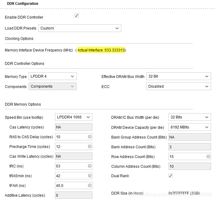
The MPSoC on Ultra96 is the XCZU3EG-1SBVA484E. This cost-optimized package supports an LPDDR4 maximum interface rate of 1066 Mbps. Therefore, the ideal clock rate is 533 MHz. In version 1.0 of the BDF, Vivado is instructed to automatically calculate the PLL parameters, which results in an actual output clock frequency of 525 MHz. The v1.2 BDF explicitly sets the PLL parameters to produce 533.3333 MHz. Therefore, the clock period tCK = 1.875 ns.
In Vivado Block Design for Zynq UltraScale+, the DDR Configuration dialog expects several parameters in the DDR Memory Options section. These parameters can be found using the Micron LPDDR4 datasheet, knowing what the memory clock period tCK (1.875 ns) is for this particular design.
RAS to CAS Delay (cycles), abbreviated tRCD.
tRCD (ns) = MAX(18ns, 4nCK)
4nCK = 4 * tCK = 7.5ns
MAX(18ns, 4nCK) = 18ns
18ns/tCK = 9.6, so round up to 10
tRCD (cycles) = 10 cycles
Precharge Time (cycles), abbreviated tRP
Micron provides both an All Bank precharge (tRPab) and a Per Bank precharge (tRPpb). We will find the maximum.
tRPab (ns) = MAX(21ns, 3nCK)
3nCK = 5.715ns
MAX(21ns, 3nCK) = 21ns
tRPpb = MAX(18ns, 3nCK)
3nCK = 5.715ns
MAX(18ns, 3nCK) = 18ns
tRP (ns) = MAX(tRPab, tRPpb) = 21ns
21ns/tCK = 11.2, so round up to 12
tRP (cycles) = 12 cycles
Row active time, abbreviated tRAS (ns)
tRAS = MAX(42ns, 3nCK) = 42ns
ACTIVATE-to-ACTIVATE command period (same bank), abbreviated tRC (ns)
tRC (ns) = MAX{[tRAS + tRPab (with all-bank precharge)], [tRAS + tRPpb (with per-bank precharge)]}
tRAS + tRPab = 42ns + 21ns = 63ns
tRAS + tRPpb = 42ns + 18ns = 60ns
tRC (ns) = 63ns
Four-bank activate window, abbreviated tFAW (ns)
tFAW (1066 Data Rate) = 40ns
DRAM IC Bus Width (per die)
32 bits, based on the Part Number MT53B512M32D2
DRAM Device Capacity (per die, so use 16 instead of 32)
512 Meg * 16 bits = 8192 Mbits
Also shown in Table 2 as “Density per die”
Row Address Count (bits)
Table 2, x16 Row addresses for 512M32 (16Gb) device = R[14:0] = 15
Dual Rank
Yes, checked, since Table 2 Configuration for 512M32 (16Gb) device shows “32Mb x 16 DQ x 8 banks x 2 channels x 2 ranks”
The resulting preset provides an LPDDR4 configuration in the block design that looks like this in Vivado:
Ultra96 LPDDR4 Vivado Block Design Configuration
这篇关于U96_LPDDR4配置的文章就介绍到这儿,希望我们推荐的文章对编程师们有所帮助!